Tel : +86-591-86395085
 Email : sales@uni-optics.com


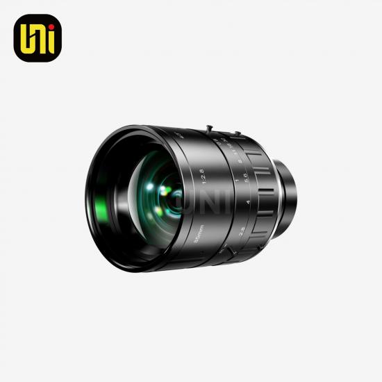
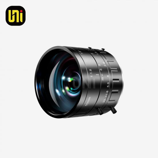
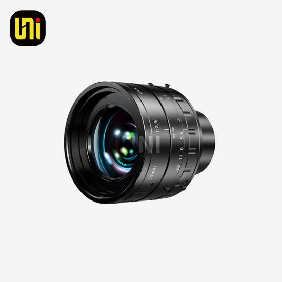
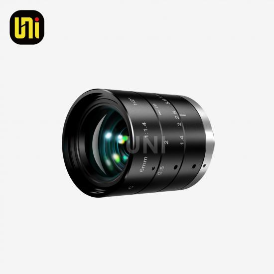
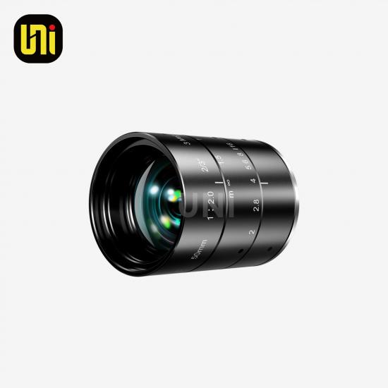
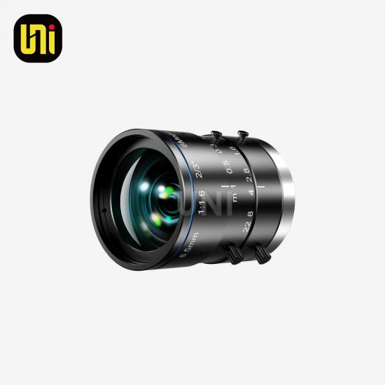
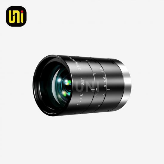
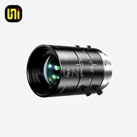
製品の特徴:
· 高い相対照度と高いコントラスト
· 低歪みと優れたコーナー輝度
· 高解像度
· 4/3インチ 45MPカメラに対応
製品情報: リクエストに応じてカスタムデザインも承ります。
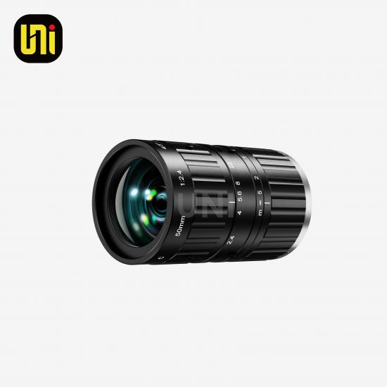
製品の特徴:
· 高い相対照度と高いコントラスト
· 低歪みと優れたコーナー輝度
· 高解像度
· 4/3インチ 45MPカメラに対応
製品情報: リクエストに応じてカスタムデザインも承ります。
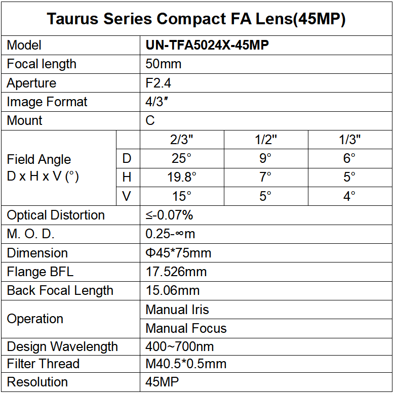
 UN-TFA2528X-45MP
製品の特徴:
· 高い相対照度と高いコントラスト
· 低歪みと優れたコーナー輝度
· 高解像度
· 4/3インチ 45MPカメラに対応
製品情報: リクエストに応じてカスタムデザインも承ります。
 UN-TFA3520X-45MP
製品の特徴:
· 高い相対照度と高いコントラスト
· 低歪みと優れたコーナー輝度
· 高解像度
· 4/3インチ 45MPカメラに対応
製品情報: リクエストに応じてカスタムデザインも承ります。
 UN-ALS284K
製品の特徴:
· 32mmビッグフレームセンサー用に開発
· 大口径、最大F2.4· 優れた光学性能、中心部と周辺部の均一な画像
製品情報: リクエストに応じてカスタムデザインも承ります。
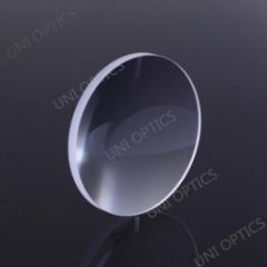 UV溶融石英平凸(pcx)レンズ
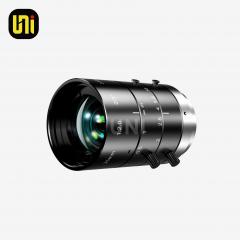 UN-TFA2520C
製品 マウサー特徴:
1. 2 / 3 ''フォーマットセンサー
2 超小型 設計
3。 ..超低歪み
4 高い相対照明
5. ..高コストパフォーマンス
6. ..フォーカスとアイリスのロックを備えています。
製品 情報: カスタムデザインがあります リクエスト
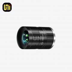 UN-TFA3524L-12MP
製品の特徴:
· 高い相対照度と高いコントラスト
· 低歪みと優れたコーナー輝度
· 高解像度
· 互換性のある1.2インチ12MPカメラ
製品情報: リクエストに応じてカスタムデザインも承ります。
 Line Scan Lens UN-ALS1164L-16K
For high-end PCB AOI inspection, Mini/Micro LED panel micro-defect detection, photovoltaic silicon wafer EL hidden crack inspection, narrow precision metal strip flaw detection, luxury printing anti-counterfeit texture inspection, electronic ceramic substrate microscopic inspection and high-precision linear dimension measurement of tiny electronic components.
· Developed for 66mm big frame sensor
· Low distortion
· Compatible for 16K line scan camera
· Excellent optical performance, uniform imaging of center and edge
Product information: Custom designs are available upon request.
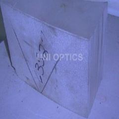 紫外線溶融シリカ